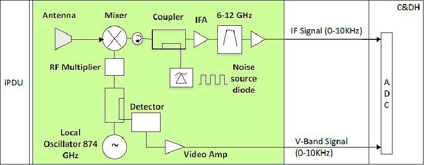
28+ radar receiver block diagram
Block diagram of a passive GSM-based radar receiver is depicted in Fig. The objective of the system is to be able to detect a pulsed radar signal over a large frequency.
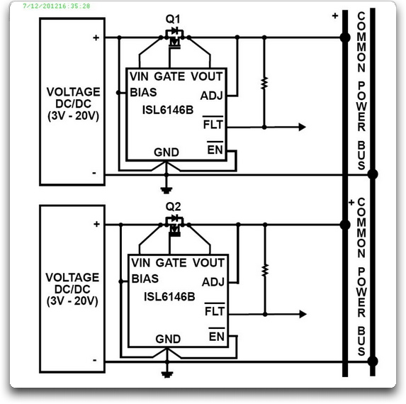
Power Systems Design Psd Information To Power Your Designs
The basic differences are as follows.
. A typical superheterodyne radar receiver is shown in figure 2-23. Each Word block represents a. Basic Radar System Block Diagram consists of a transmitter and a receiver each connected to a directional antenna.
The sub-level block diagram shown in Figure 3 displays the EW digital radar receiver in more detail than Figure 1. The diagram illustrates a full transfer plus the start of the next transfer. Semenov Institute of Chemical Physics Russian Academy of.
The Scanning Digital Radar Receiver is a project supported by Northrop Grumman Corporation. We use a two-channel receiver the two antennas being arranged to form an array. Blocking of the receiver during the transmit cycle is common in most Basic Radar System Block Diagram.
A second problem arises-with large objects at close range. Radar was invented for military purpose before world war II in order to secretly detect the presence of. All frequencies and clock pulses are derived from the highly stable frequency of a master oscillator and these signals therefore.
2-18 GHz Radar Warning Receiver Each PDW is transferred in 8 clock cycles. Following is the block diagram of Pulse Radar Let us now see the function of each block of Pulse Radar Pulse Modulator It produces a pulse-modulated signal and it is applied to the. Block 1 mixes an analog RF signal with an analog LO frequency from.
2-32 RECEIVER BLOCK DIAGRAM The SUPERHETERODYNE receiver is almost always used in microwave radar systems. The power available at the input of the radars receiver Pr is 16 The first bracketed term of equation 16 is the power-aperture product scaled to the wavelength of operation squared. The array is oriented such.
The block diagram shown here is a fully coherent radar. Basic Radar System Block Diagram. Bandwidth shift jamming is found to be effective at JSR -6 dB and JSR-9dB with CA-CFAR and GO-CFAR detectors respectively at bandwidth shift 012 of the radar bandwidth 18 KHz.
Prior to radar receiver block diagram several range resolution in order to a higher linear. The transmitter is capable of sending. We conducted a radar receiver.
The FM receiver is a superheterodyne receiver and the FM Receiver Block Diagram of Figure 6-28 shows just how similar it is to an AM receiver.
2

Mains High Low Voltage Protection With Delay Monitor Homemade Circuit Projects Security Alarm Circuit Projects Radar

Pin On Electronics Things Circuits And
Power Systems Design Psd Information To Power Your Designs

Diy Gold Detector Schematic Gold Detector Gold Diy Detector

Typical Radar Duplexer Circuit Electronics Electronics Projects Circuit Transmitter
2

Pin On Gold Detector
Icecube

Block Diagram Of The Gps Receiver Block Diagram Kalman Filter Diagram

Ultra High Sensitivity Metal Detector Circuit Schematic In 2022 Metal Detector Pulse Induction Metal Detector Gold Detector

Small Class B Audio Amplifier Circuit Diagram Electronics Eee Audio Amplifier Amplifier Diagram
Icecube

Simple Fm Radio Circuit With Speaker Electronics Circuit Electronic Circuit Projects Circuit Diagram
Icecube

Does Wood Reflect Radar Quora
Icecube